
18·
2 years ago- Todd the Father
- Todd the Son
- Todd the Spirit
Yes, there will be progress but that’s not really what Moore’s Law is about. Moore’s Law is not an observation that there will be progress eventually but an observation at specific rate of that progress. It’s not “transistors will double eventually”, or “transistors will increase somewhat every 2 years”.
With exponential growth, the tiniest decrease compounds to a major difference. 2 to the power of 3 is 8; the A16 has 16B transistors not 26B. That’s with the gains of the last DUV nodes, 16->10->7nm. EUV to EUV, 5nm to 3nm doesn’t match up to that. It seems transistor growth with EUV nodes is becoming linear so not really in line with the exponential growth of Moore’s Law.
The chips could be larger but flagship phones would have to become even more expensive, and physically larger to dissipate the extra heat. Dennard Scaling mattered more in practice than Moore’s Law ever did but that ended over a decade ago. At the end of the day, all the microarchitecture and foundry advances are there to deliver better performance for every succeeding generation and the rate of that is definitely decelerating.
In 3 years, the only Android chip that has a perceivable difference in performance from the Kirin 9000 is the 8 Gen 2, which cost $160 just for the chip. That performance difference isn’t even enough to be a selling point; the Mate 60 Pro is in the same price range as those 8 Gen 2 phones yet is still perfectly competitive in that market segment.
Transistor density isn’t doubling every 2 years.
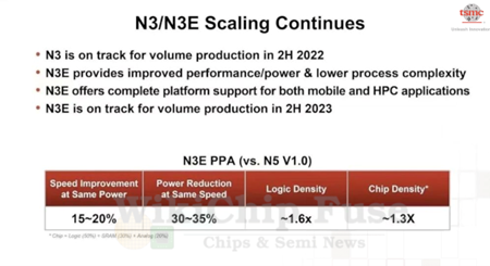
N3E is only 1.6x denser than N5 and that only apply to logic transistors. TSMC assumes logic makes up 50% of a hypothetical chip to arrive at 1.3x scaling. It wouldn’t come anywhere near close to actually doubling in real chips.
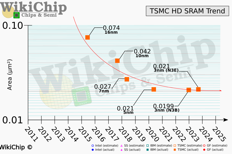
Analog and SRAM scaling has been decelerating for years. TSMC N3E has the same SRAM cell size as N5. Samsung 4nm has the same SRAM cell size as 7nm. Because they don’t scale with logic, every succeeding generation these components will take up more and more of the silicon hence AMD’s move to chiplets.
Men of War
Red Faction Guerilla
Just copy all the contents of the SD card over to be safe. Retroarch might be storing files on the SD card and the BIOS folder might be separate from the ROMs.
Having firmware on the SD card is unique to Linux handhelds. Android handhelds are basically phones so the operating system is in the flash chip on the motherboard.

The only Nintendo console I ever had was a Famiclone so I don’t really have much nostalgia for their games.
It’s just Nintendo ROMs that are disappearing. It’s still easier than ever to find even the most obscure classic PC games on abandonware sites and GOG compilation torrents. It’s also only the SEO abusing ROM sites that are vulnerable to Nintendo’s attacks. Complete ROMsets for their consoles can still be obtained through torrents, Vimm.net, and the r/ROMs megathread especially for the older cartridge consoles.
Emulating a current gen Nintendo console has never been as good as it is for Switch emulators. Any new PC can emulate Switch Triple As at full speed. Android is getting builds of the Yuzu emulator and mobile SOCs have enough power to run less demanding titles. When a lot people who don’t even own a Switch can play Tears of the Kingdom, Nintendo is understandably trying to crack down. The portable aspect of the Switch is no longer a unique advantage. It used to be just GPD making those handheld PCs now every brand is trying to compete in that form factor.
Honestly I think the state of emulation in general is experiencing a golden age.
Retroid, Anbernic and AYN are making hardware that is a better solution for most people than trying to jailbreak and refurbish old original portable consoles. The screens, the analogs and the buttons they use are as good if not better than the first party hardware. Unlike bulky handheld PC, their Linux or Android based emulation handhelds are still in the same size and weight class as the PSP.
A couple years ago the Xbox 360 and PS3 emulators were basically just experimental demos. They weren’t stable enough to actually finish any game on and most CPUs weren’t fast enough to run them at full speed. They’re still hit and miss but the list of playable titles will only ever grow.
It has come to the point that the PC can play everything. All previous gen consoles aside from the OG Xbox have emulators at a playable state. There are almost no current gen console exclusives anymore as the PC is getting ports of PS4/PS5 exclusives, the XBone/Series never had any to begin with, and of coarse the aforementioned Switch emulation.

That’s based on TSMC’s own test chip not an actual customer’s. 17.92 mm² is incredibly tiny when SoCs, CPUs and GPUs range in size from 100 to 600 mm² increasing the proportion of chips with defects as the number of chips on the wafer drops.
From that very article
In that case, let us take the 100 mm2 die as an example of the first mobile processors coming out of TSMC’s process. Again, taking the die as square, a defect rate of 1.271 per cm2 would afford a yield of 32.0%.
As TSMC themselves designed the chip, they definitely followed all their design rules for that process to maximize yield. No customer would do that.
Anand explains this in one of his articles.
But have no fear. What normally happens is your foundry company will come to you with a list of design rules and hints. If you follow all of the guidelines, the foundry will guarantee that they can produce your chip and that it will work. In other words, do what we tell you to do, and your chip will yield.
The problem is that if you follow every last one of these design rules and hints your chip won’t be any faster than it was on the older manufacturing process. Your yield will be about the same but your cost will be higher since you’ll bloat your design taking into account these “hints”.
Generally between process nodes the size of the wafer doesn’t change. We were at 200mm wafers for a while and now modern fabs use 300mm wafers. The transistor size does shrink however, so in theory you could fit more die on a wafer with each process shrink.
The problem is with any new process, the cost per wafer goes up. It’s a new process, most likely more complex, and thus the wafer cost is higher. If the wafer costs are 50% higher, then you need to fit at least 50% more die on each wafer in order to break even with your costs on the old process. In reality you actually need to fit more than 50% die per wafer on the new process because yields usually suck at the start. But if you follow the foundry’s guidelines to guarantee yield, you won’t even be close to breaking even.
The end result is you get zero benefit from moving to the new process. That’s not an option for anyone looking to actually use Moore’s Law to their advantage. Definitely not for a GPU company.
The solution is to have some very smart people in your company that can take these design rules and hints the foundry provides, and figure out which ones can be ignored, and ways to work around the others. This is an area where ATI and NVIDIA differ greatly.
TSMC N7, N7P and Intel 7 don’t use EUV. It’s all quad patterned DUV. DUV lithography has been in use since the 1990s going from 800nm to N7P.
Every single node after TSMC’s so called 16nm has been all marketing. It would’ve more accurate to call TSMC 16FF as 20nm FinFET. This is why Intel brands what they themselves called 10nm as Intel 7 to bring their marketing more in line with TSMC’s.
SMIC N+1 has a density of 89 million of transistors per mm² while TSMC N7 has 91.2. TSMC 10FF and Samsung 10LPP only offer slightly more than half that density.
Well the typical maritime disaster back then had far more resemblance with that of the SS Arctic’s sinking, which had no surviving women and children no matter their status. It’s the crew that’s most likely to survive. The women and children were the most likely to perish. Every man for himself was indeed the norm, which is why the Titanic seemed special. It’s more down an individual’s survival skills, whether they were stationed/staying in the safest parts of the ship, and in some cases even their willingness to screw other people over in order to survive.
Gender, Social Norms and Survival in Maritime Disasters by Mikael Elinder, Oscar Erixson
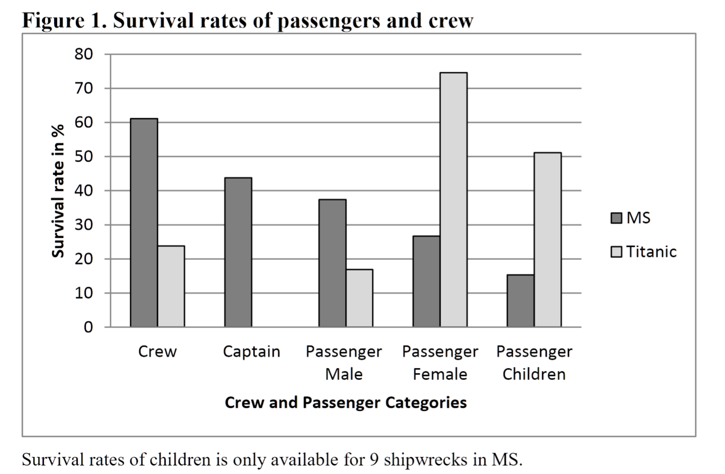
Our results provide new insights about human behavior in life-and-death situations. By investigating a new and much larger sample of maritime disasters than has previously been done, we show that women have a substantially lower survival rate than men. That women fare worse than men has been documented also for natural disasters (32-36). We also find that crew members have a higher survival rate than passengers and that only 7 out of 16 captains went down with their ship. Children appear to have the lowest survival rate.
Moreover, we shed light on some common perceptions of how situational and cultural conditions affect the survival of women. Most notably, we find that it seems as if it is the policy of the captain, rather than the moral sentiments of men, that determines if women are given preferential treatment in shipwrecks. This suggests an important role for leaders in disasters. Preferences of leaders seem to have affected survival patterns also in the evacuations of civilians during the Balkan Wars (37).
Moreover, we find that the gender gap in survival rates has decreased since WWI. This supports previous findings that higher status of women in society improve their relative survival rates in disasters (35). We also show that women fare worse, rather than better, in maritime disasters involving British ships. This contrasts with the notion of British men being more gallant than men of other nationalities.
Finally, in contrast to previous studies, we find no association between duration of the disaster and the influence of social norms. Based on our analysis, it becomes evident that the sinking of the Titanic was exceptional in many ways and that what happened on the Titanic seems to have spurred misconceptions about human behavior in disasters.
I got the original picture from what is apparently a Forbes ad campaign by Goodby Silverstein.
Russia’s officially stated original goal was basically the Minsk accords, but instead of autonomy it was changed to independence for Donbass.
Ukraine officially stated goal is Crimea and Donbass.

